Fundamentals of Device and Systems Packaging
The Importance of Efficient Packaging in Modern Devices and Systems
Device and systems packaging is a critical aspect of modern technology that often goes unnoticed by the end users. Packaging plays a crucial role in ensuring the reliability, performance, and longevity of electronic devices. In this blog post, we will delve into the fundamentals of device and systems packaging and explore why it is essential for the functionality of various electronic products.
Understanding Device and Systems Packaging
Device and systems packaging involves the design and fabrication of protective enclosures for electronic components, ensuring that they are shielded from environmental factors such as moisture, dust, and mechanical stress. Packaging also encompasses the integration of various components into a cohesive system, optimizing space utilization and thermal management.
One of the key considerations in device packaging is the selection of materials that offer a balance between durability, conductivity, and thermal properties. For example, advanced polymers and ceramics are often used in semiconductor packaging to provide electrical insulation and heat dissipation.
The Evolution of Packaging Technologies
Over the years, packaging technologies have evolved significantly to meet the demands of shrinking device sizes and increasing performance requirements. Miniaturization has led to the development of advanced packaging techniques such as system-in-package (SiP) and chip-on-board (COB), enabling the integration of multiple functions into a single package.
Furthermore, the use of flip-chip packaging has revolutionized the semiconductor industry by allowing for enhanced signal integrity and faster data transfer rates. Through innovations in fan-out wafer-level packaging (FOWLP) and 3D stacking, manufacturers can now achieve higher levels of integration and performance in compact form factors.
Challenges and Solutions in Device Packaging
Despite the advancements in packaging technologies, engineers face several challenges when designing and fabricating device packages. Issues such as solder joint reliability, thermal management, and electromagnetic interference (EMI) can significantly impact the performance and reliability of electronic devices.
To address these challenges, researchers are exploring novel packaging solutions such as embedded cooling systems, conductive adhesives, and electromagnetic shielding materials. By incorporating these innovations into device packaging, manufacturers can enhance the efficiency and robustness of electronic systems.
Future Trends in Device Packaging
Looking ahead, the future of device packaging is likely to be shaped by emerging technologies such as internet of things (IoT), artificial intelligence (AI), and 5G connectivity. These trends will drive the demand for smarter, smaller, and more energy-efficient devices, necessitating innovative packaging solutions.
Key areas of focus for future device packaging include flexible and stretchable electronics, bio-compatible materials, and environmentally sustainable packaging practices. By leveraging advances in materials science, nanotechnology, and additive manufacturing, engineers can develop next-generation packaging solutions that meet the evolving needs of the electronics industry.
Conclusion
In conclusion, device and systems packaging is a critical enabler of modern technology, influencing the performance, reliability, and form factor of electronic devices. By understanding the fundamentals of packaging technologies and staying abreast of emerging trends, engineers can develop innovative solutions that drive the next wave of technological advancements.


-
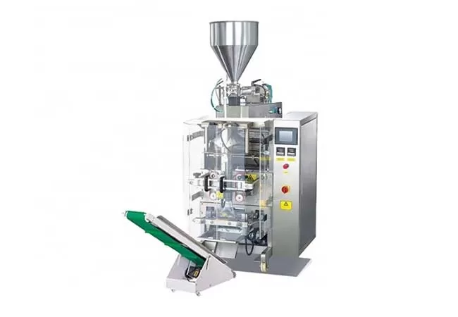
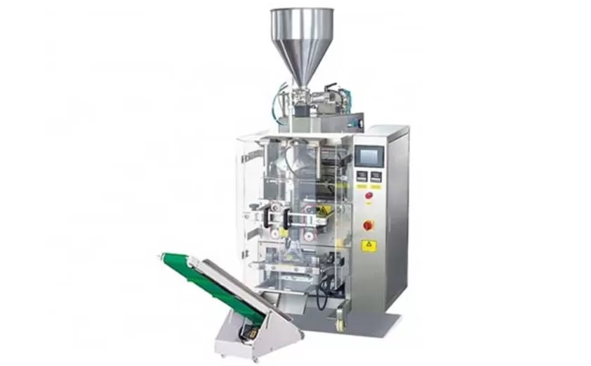
VFFS Equipment: The Ultimate Guide to Vertical Form Fill Seal Technology
13-03-2026 -
The Essential Guide to Weight Packing Machines for Precision Weighing
12-03-2026 -
Power Packing Machine: The Ultimate Guide to Heavy-Duty Packaging Efficiency
11-03-2026 -
Weigher Packing Machine: The Definitive Guide to Precision Weighing & Packaging
10-03-2026 -
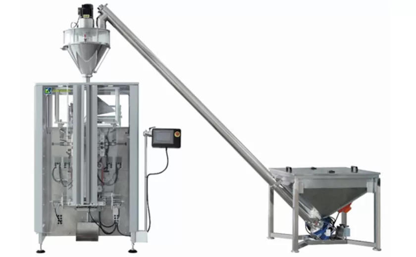
Auger Type Powder Filling Machine: The Ultimate Guide to Precision Packaging
09-03-2026 -
Advanced Packing Solutions: Snacks, Sugar, and Frozen Food Machines
29-10-2025 -
Efficient and Reliable Solutions for Salt, Nuts, and Frozen Dumplings Packing
29-10-2025 -
High-Performance Biscuits, Lollipop, and Ketchup Packing Machines for Modern Food Production
29-10-2025 -
Efficient Liquid Filling and Packing Machines for Modern Production
23-10-2025 -
Reliable Granule Packaging Machines for Efficient Production
23-10-2025
